Many embedded signal-processing systems require good energy efficiency. Some devices, such as medical implants and wireless sensors, must operate for years on just one battery charge. To do so, these devices must consume only microwatts of power—a significant design challenge to say the least! Larger devices such as cellular phones and multimedia-oriented PDAs can afford larger batteries and higher energy consumption, but they also must support heavy processing loads. Today's cellular phone designers, for example, must pack multiple processors, backlit color displays, several wireless communication interfaces, megabytes of memory, and a host of other bells and whistles into a small and lightweight package. And all of this must run for many hours on a diminutive one-ounce battery. Even line-powered devices such as industrial controllers and health monitors can have tight energy budgets due to heat dissipation or power-supply constraints.
Technology improvements, such as low-voltage chips, help reduce energy consumption for a given set of system features and level of performance. But system features and performance are moving targets: typically, with each product generation designers must integrate additional energy-consuming features and deliver even higher performance in an ever-shrinking space. This creates an energy efficiency crunch. And, unfortunately, battery technologies tend to improve at a maddeningly slow pace compared to other electronic technologies. As shown in Table 1, the latest lithium ion batteries offer only a three-fold improvement in storage density over nickel cadmium batteries—which were invented in 1899!

A variety of design techniques can reduce energy consumption in a signal processing system. These range from new low-power chip fabrication techniques to energy-aware software design. Although many of the ideas covered in this article are applicable to a broader range of low-power electronic systems, we focus on techniques for processor-based embedded systems aimed at signal processing-intensive applications.
Low-Power Chip Design
Processors, memories, and other silicon components consume a significant portion of the total system energy in a typical battery-powered device. Thus, they are an obvious place to start when beginning to optimize a design for low energy consumption.
The dominant digital chip fabrication technology is CMOS—complimentary metal oxide semiconductor. One interesting feature of a CMOS logic gate is that it consumes very little energy when idle. In contrast, when a CMOS logic gate transitions between states (for example, switching from 0 to 1) it consumes much more energy. This means that designers can save lots of energy if they can keep the majority of a CMOS chip inactive. (As we discuss later, this situation is changing with the latest emerging fabrication processes, where idle power consumption is becoming a much larger factor.)
Calculating CMOS Power
A simplified equation for power consumption in a CMOS gate is P = CLV2f + IqV, where CL is the load capacitance, V is the supply voltage, Iq is the leakage current, and f is the switching frequency.
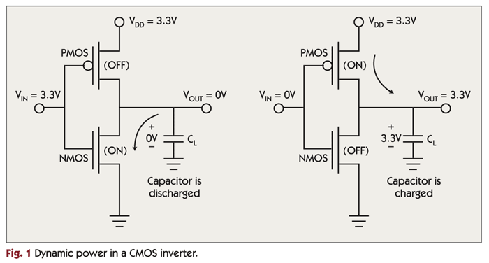
The first part of the equation, CLV2f, describes the dynamic power that is dissipated in a CMOS gate as it switches. To illustrate this concept, Figure 1 shows a diagram of two CMOS inverters, one with an input of 3.3 volts, the other with an input of 0 volts. The output of an inverter is the "opposite" of the input: each time the input voltage switches from 3.3 to 0 volts, the output switches correspondingly from 0 to 3.3 volts. Energy is consumed primarily when the output switches. Any CMOS gate has a load capacitance CL associated with its output. Driving this load capacitance from 0 to 3.3 volts requires energy and this is where dynamic CMOS power is consumed.

The first thing to notice about the equation P = CLV2f + IqV is that power consumption varies linearly with frequency. If the leakage current Iq is relatively small, reducing the operating frequency of a typical CMOS chip by a factor of two also reduces the power consumption by about a factor of two. More importantly, though, notice that the first voltage term of this equation is squared. This implies that if the supply voltage can be reduced, this also has a significant effect on power consumption. Unfortunately, driving a CMOS chip at lower voltages also means that its maximum operating frequency is reduced, which in turn results in lower performance. Thus, when attempting to optimize battery life, designers must carefully weigh the performance consequences of reduced voltage and chip frequency.
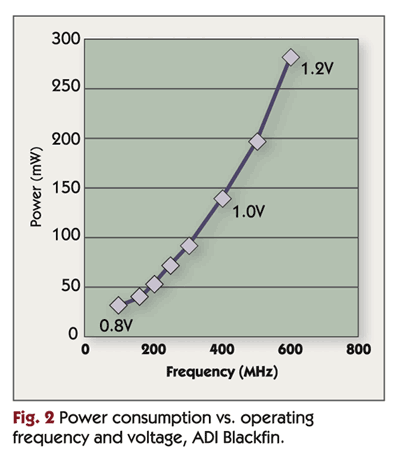
Figure 2 shows the combined effects of frequency and voltage on power consumption in the Analog Devices Blackfin DSP. Notice the quadratic shape of the curve due to the change in voltage.

Technology Improvements Lead to Headaches
In a typical CMOS fabrication process, the leakage current Iq tends to be negligible and thus has traditionally been ignored by designers. Leakage current comprises the static component of CMOS power consumption (IqV), as opposed to the dynamic component (CLV2f). It is "static" in the sense that this power is consumed even when chip activity is zero (f = 0). Unfortunately, leakage current cannot be ignored for much longer. As CMOS fabrication technology improves by shrinking distances between chip features, leakage current increases dramatically because electrons can literally leak into layers of material that are supposed to be insulating. Today, most chips use 0.25- and 0.18-micron CMOS technology. As the semiconductor industry transitions to smaller and faster 0.13- and 0.09-micron (90 nanometer) CMOS, the required supply voltage goes down and the achievable frequency goes up, but leakage current grows. When we reach 65 nm and 45 nm CMOS technology in a few years, some experts believe that the leakage current will be so high that IqV will account for as much as 50% of total chip power consumption.
Leakage current is not the only problem on the horizon as CMOS technology advances. Shrinking geometries mean that far more transistors can be packed onto one chip, and transistor counts will undoubtedly increase to meet demands for increased performance and integration. Unfortunately, as transistor count and overall chip complexity go up, the load capacitance CL tends to increase due to increased interconnect lengths and fan-out density, which drives up dynamic power consumption. In addition, clock frequencies are continually increasing in order to satisfy performance-hungry signal processing applications.
A Triple Whammy
The combination of higher leakage current, more transistors per chip, and higher clock speeds means that chip and system designers can't assume that chips will become more energy efficient as they move to more advanced fabrication processes. Hence, chip designers and manufacturers are employing a number of techniques to improve chip energy efficiency. For example, most foundries now offer CMOS gate libraries that are optimized for very low-voltage operation (1 volt or less). Not only does lower voltage lead to lower dynamic power consumption, it also helps to reduce leakage current in a CMOS transistor because a lower voltage is applied across insulating layers, giving electrons a lower potential to leak through these layers. Unfortunately, though, chips that are fabricated using ultra low-voltage libraries tend to be limited to lower speeds.
New Tricks of the Trade
One obvious low-power technique is to simply turn off power to inactive areas of the chip. In many designs, only a small fraction of a chip is active at any given time, so significant gains can be made by partitioning a chip into multiple power domains and only maintaining power in the active areas. In the past, it was sufficient to simply remove the clock to the inactive areas (thus removing the dynamic component of power consumption). But with increasing losses due to leakage current, designers must now consider turning off the power as well.
While it sounds simple to "turn off" inactive areas of a chip, in practice this involves a number of design challenges. For example, it's difficult enough to design and verify a complex chip with just a few power and clock domains. Adding additional domains to support power management means that chip designers must implement many more domains and verify correct operation even when the majority of the chip has no power. Moreover, some parts of a chip may require information to be saved elsewhere when power is removed and properly restored when power is brought back.
A related technique is to partition a chip into multiple "voltage islands." By using this technique, designers can supply a reduced voltage to each area of the chip according to its speed requirements.
Because leakage current is becoming such a menacing problem, a number of other techniques are being developed to combat it. For example, some foundries now offer CMOS transistor libraries with a range of threshold voltages. Transistors with low threshold voltages offer fast switching speeds, but also have much higher leakage currents. By giving designers a choice between faster, high-leakage transistors and slower, low-leakage transistors, the overall leakage current can be minimized for a given design while minimizing the impact on speed-critical portions of the chip. Another technique called "back-biasing" allows threshold voltages to be dynamically tuned for a given area of a chip. This works by applying a bias voltage to transistors that allows threshold voltages (and thus leakage) to be raised or lowered dynamically through on-chip control logic.
New Tools and Processes
Recent dramatic advancements in IC fabrication technology, such as strained silicon-on-insulator (SSOI) processes, promise to revolutionize the industry by increasing performance and reducing energy consumption with only moderate increases in fabrication costs. SSOI and related technologies work by literally "stretching" the underlying silicon lattice, which enhances the ability of electrons to flow. In addition, because parts of the transistor are buried in an insulating layer, both leakage current and parasitic capacitance are reduced, contributing to lower energy consumption.
Last but not least, new advancements in design automation tools promise to aid the low-power chip designer. IC design tool vendors have been scrambling to develop power-aware tools that can help designers accurately estimate power consumption, identify hotspots that are ripe for power optimization, and implement multiple power and clock domains.
Processor Power-Saving Techniques
In the previous section we explored a variety of chip design techniques that can be used to reduce energy consumption. But what if—like most system designers—you're not designing your own chips, yet need to maximize energy efficiency? There are many other energy-efficient design techniques that can be applied at the processor, system, and software level. All of these can have a profound impact on energy consumption. In this section we explore processor power-saving techniques; in later sections we investigate system and software techniques.
Processor Idle Modes
Manufacturers of embedded microprocessors and DSPs have introduced a variety of power-saving features into their products. The most common feature is a low-power "sleep" mode. For example, when a handheld device has finished all pending work and is waiting for user input or a scheduled event, the operating system can turn off the processor's core clock while maintaining the clock signal to its on-chip peripherals and memory. When the user provides a new input to the system, the processor can awaken within milliseconds and process the input quickly enough that the user doesn't notice the wake-up delay. Table 2 shows the five available sleep modes of the Analog Devices Blackfin DSP family.

"Deeper" idle modes can place the processor into a more aggressive low-power state, at the cost of a longer wake-up latency. For example, a processor could stop all on-chip peripherals and even the clock generator PLL, using just enough power to maintain the contents of on-chip memory. It takes much longer to wake up from such a mode because the PLL cannot be restarted instantaneously. (Refer to "Processor Power Consumption: Beyond the Data Sheet" for further discussions of processor wake-up delay.)
Voltage and Speed Adjustments
An increasingly common feature among the latest processors is the ability to dynamically adjust frequency and core voltage (the main supply voltage for the processor) through software control. By supporting a range of voltages and frequencies, power consumption can be dynamically reduced based on the computational load. For example, an MP3 player application on a high-end PDA does not tax the processor significantly. If the processor supports dynamic voltage scaling, the processor clock speed can be turned down (perhaps to 20% of its maximum clock speed), which in turn allows the processor core to be operated at a lower supply voltage. When more demanding applications are loaded (such as MPEG-4 video decoding), the processor can be restored to full speed.
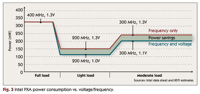
Today's processors generally achieve the best energy efficiency on a given task if they are run at the lowest voltage and speed necessary to complete that task. This results in the highest energy efficiency because it minimizes the dynamic CMOS power component, CLV2f. At higher speeds, the processor requires higher voltage and thus exhibits reduced energy efficiency. For example, the Intel PXA255 consumes 0.80 mW/MHz when operating at 400 MHz and 1.3 volts, but it consumes only 0.58 mW/MHz when operating at 200 MHz and 1.0 volts. By choosing the appropriate speed and voltage settings for each task, designers can maximize energy efficiency. Figure 3 demonstrates how designers can optimize the Intel PXA255 power consumption by adjusting its voltage and frequency according to processor load.

While the energy efficiency versus speed relationship illustrated in Figure 3 may be representative of most embedded processors today, the situation may reverse in the near future. Advancements in CMOS fabrication processes (and corresponding increases in leakage current) will cause static power consumption to increase significantly when the processor is in an active mode. Once these new fabrication processes become common, many processors will be most energy efficient when run at full speed and voltage for the minimum length of time necessary to handle the workload and then will transition to a sleep state where leakage is minimized.
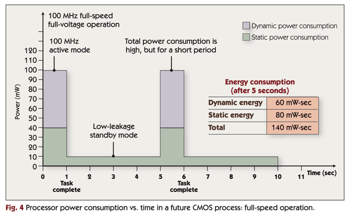
Figures 4 and 5 illustrate two power consumption profiles for a hypothetical processor implemented in a future CMOS process. In both figures, the load is a periodic task that repeats every five seconds. Figure 4 shows a "full-speed" profile where the processor performs the task at its top speed and voltage and then enters a low-leakage standby mode. Figure 5 shows a "reduced-speed" profile where the processor performs the task at a lower speed and voltage. In this second scenario, the processor spends less time in standby mode.

As shown in the figures, the second scenario has higher overall energy consumption, despite running at a lower voltage and speed. In the second scenario, the processor is in active mode for a longer period of time. As a result, the processor has higher active-mode static energy consumption. In fact, active-mode static energy consumption dominates the overall energy consumption in the second scenario.
Other Features
A number of other processor features can help to reduce power consumption. For example, many processors include special-purpose coprocessors that can perform computationally intensive tasks using far less energy than would be consumed by software implementations of these tasks. This is especially beneficial for multimedia tasks such video compression. (Refer to "Processors for Low-Power Signal Processing" for more information on architecture-related aspects of low-energy processors.)
Reducing System Power Consumption
Perhaps the most effective technique for reducing system power consumption is to dynamically turn off unused peripherals, LCD backlighting, wireless communications transceivers, and memories whenever possible. The ability to do this, however, depends both on the capabilities of the individual components and also the ability of the operating system to place inactive peripherals in a low-power state in an intelligent fashion.
Integration Is Key
One key for designing a low-power embedded system is component integration. Not only does a low chip count and a small printed circuit board lead to lower cost and physically smaller devices, it can also help to dramatically reduce power consumption. When signals propagate within a chip, they experience minimal signal loss because the wires are extremely short and the loads are very small. On the other hand, signals that must be driven off-chip must travel a much longer distance and must drive much larger loads. Thus, to minimize energy consumption, whenever high-bandwidth communication must take place between two components, it is best to integrate the two components into one chip. From a power consumption perspective, the most important components to integrate are typically the processor and memory due to their high-frequency interaction.
Low-Power Wireless
In a typical wireless handset, the wireless components such as the power amplifier, transceiver, and baseband processor can consume over half of the PCB area and a significant fraction of total power consumption. A recent trend in low-power design for wireless communications is to implement significant portions of these wireless components in digital CMOS logic rather than traditional analog technologies such as SiGe. Whenever RF components can be implemented in digital CMOS, many of the benefits of improved CMOS fabrication processes (which tend to improve faster than analog process technologies) can then be applied to the RF side as well. For more information on trends in wireless devices, see "Long Live the Battery: Low-Power Signal Processing Trends."
Low-Power Software Techniques
So far we've discussed chip, processor, and system techniques for reducing power consumption. The final set of techniques we cover are in the realm of software design.
Software can have a significant impact on energy consumption. Software that is efficient in terms of the number of processor cycles required to perform a task also tends to be energy efficient. Low cycle counts mean the processor can either operate in a lower-speed, lower-voltage mode or can enter a low-power standby mode more quickly. Thus, optimizing critical inner loops of signal processing code often results in reduced energy consumption.
Taking advantage of run-time power management features such as low-power processor idle modes require software that can take advantage of such features. Unfortunately, making use of low-power modes and features can be difficult. For example, some processors offer the ability to dynamically change core voltage and frequency thousands of times per second under software control. Efficient use of this feature requires the ability to quickly and accurately measure computational load on a millisecond-by-millisecond basis, a daunting task for some applications. However, for other applications it is possible to accurately characterize load at design time, which simplifies the use of power management features and offers an excellent opportunity to optimize algorithm software for energy efficiency.
Many other software techniques can be employed to reduce power consumption. For example, when an embedded operating system manages many concurrent tasks, the intelligent scheduling of processor and other resources can lead to reduced power consumption. Instead of frequently waking up an idle processor to perform low-priority tasks, software can be written so that low-priority tasks are delayed until a higher-priority task must be performed. Because extra energy is required to wake up an idle processor, this amortizes the power consumption of waking up the processor over several tasks.
Another important software technique for reducing energy consumption is minimizing processor accesses to off-chip memory. As mentioned earlier, the power required to access off-chip memory is usually much higher than that used for accessing on-chip memory. Signal processing algorithms tend to have fairly predictable behavior, and this can be exploited to reduce off-chip memory access. For example, one basic technique is to keep frequently used constants and data in registers or on-chip memory. Another technique is to preload blocks of algorithm data into on-chip memory using DMA transfers, rather than access one word at a time from off-chip memory. In some cases, it may be possible to restructure algorithm loops so that data can be accessed in contiguous groups rather than by jumping around the address space. This is advantageous for burst-oriented memory such as SDRAM, where as many as eight contiguous words of memory are transferred even if the processor only needs one of these words. One final technique is to restrict memory access by a software module to a single bank of external SDRAM, which may allow other SDRAM bank arrays to remain in a lower-power mode for longer periods.
Conclusion
Fundamentally, digital signal processing is all about analyzing and synthesizing physical signals. These signals may be associated with the human body, with a wireless communication link, with monitoring the environment, or with any of thousands of other applications. Of course, these physical signals occur everywhere and anywhere—most often, not in places where an AC outlet is available. As a result, there are huge opportunities for energy-efficient signal processing systems.
But as we've seen, designing energy-efficient signal processing systems is anything but straightforward. Energy-efficient design requires examining nearly every aspect of the system and employing appropriate optimization techniques at every level, including chip, software, and system.


Add new comment