Germany-based processor IP provider videantis, launched in 2004, was one of the first of what has since become a plethora of vision processor suppliers. The company's latest fifth-generation v-MP6000UDX product line, anchored by an enhanced v-MP (media processor) core, is tailored for the deep learning algorithms that are rapidly becoming the dominant approach to implementing visual perception (Figure 1). Yet it's still capable of handling the traditional computer vision processing functions that were the hallmark of its v-MP4000HDX precursor.

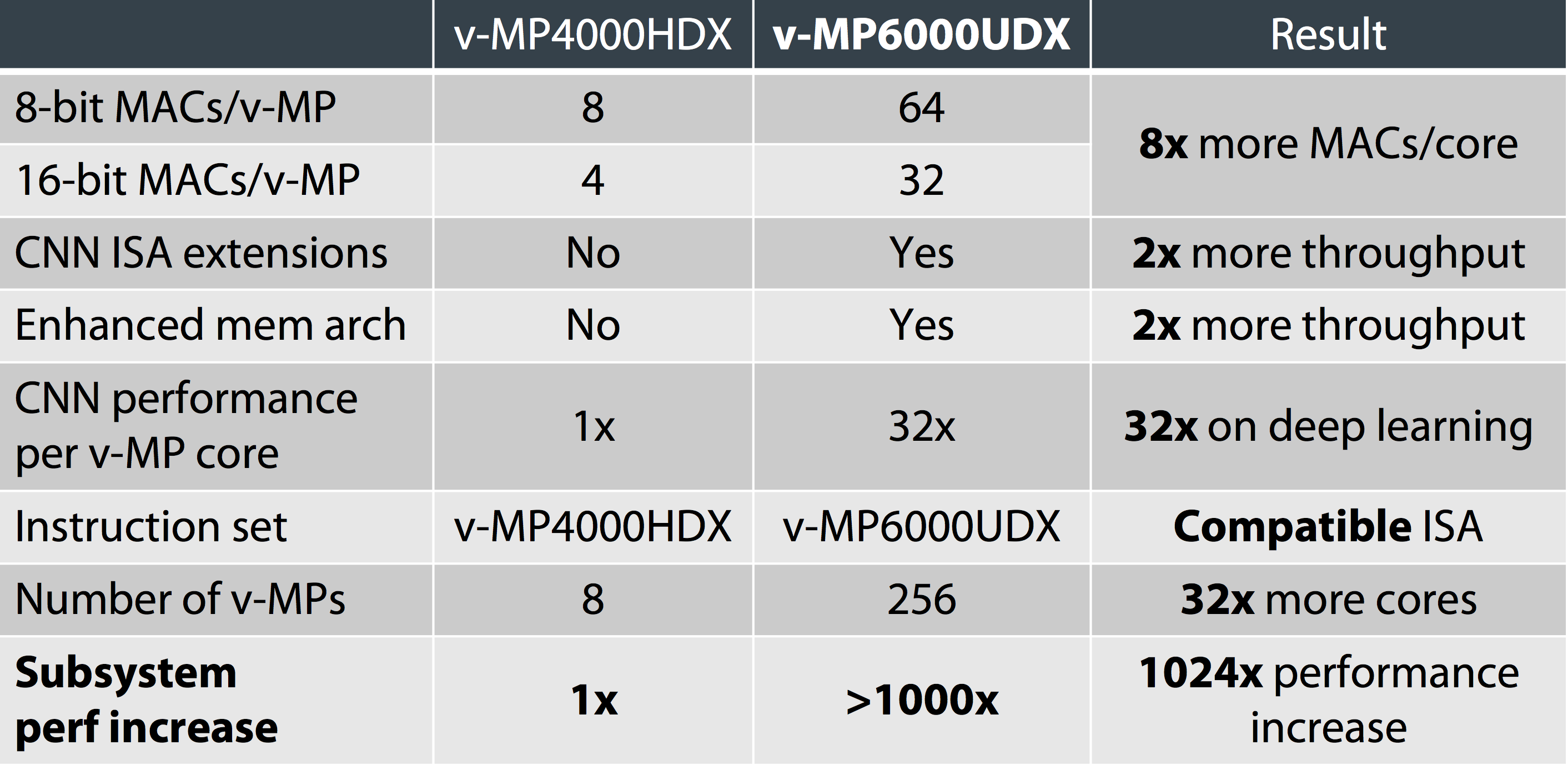
Figure 1. Figure 1. More MAC units per media processor core, along with an expanded instruction set and other enhancements, enable videantis' v-MP6000UDX architecture to more effectively tackle deep learning inference tasks.
v-MP6000UDX's v-SP (stream processor) core also retains the low-latency, bitrate-efficient video coding capabilities that were a dominant focus of the company's initial offerings, introduced more than a decade ago. Specific v-MP6000UDX implementations will encompass both varying numbers and proportions of v-MP and v-SP cores, in customizing them for particular application requirements. The planned v-MP62320UDX, for example, contains two v-SP cores for dual-channel bit stream coding capabilities, along with 32 v-MP cores.
At the foundation of the v-MP6000UDX enhancements, according to company Vice President of Marketing Marco Jacobs, is the substantial transistor budget that's cost-effectively available in modern process nodes. Jacobs believes that the bulk of his licensees' v-MP6000UDX–based SoC designs will use 16 nm or smaller lithographies. Contrast that forecast with the company's first single-core concept design, unveiled at the 2004 IEEE International Solid State Circuits Conference, which targeted a 180 nm process.
What does this higher transistor count deliver? Significantly larger numbers of MAC units per core, for one thing, a particularly beneficial attribute for doing deep learning inference. Each dual-issue VLIW v-MP core in the previous-generation v-MP4000HDX-based design includes eight 8-bit MAC units, alternatively configurable as four 16-bit MAC units. The v-MP core in the successor v-MP6000UDX architecture encompasses 64 8-bit MAC units (alternatively usable as 32 16-bit MAC units), an 8x per-core increase.
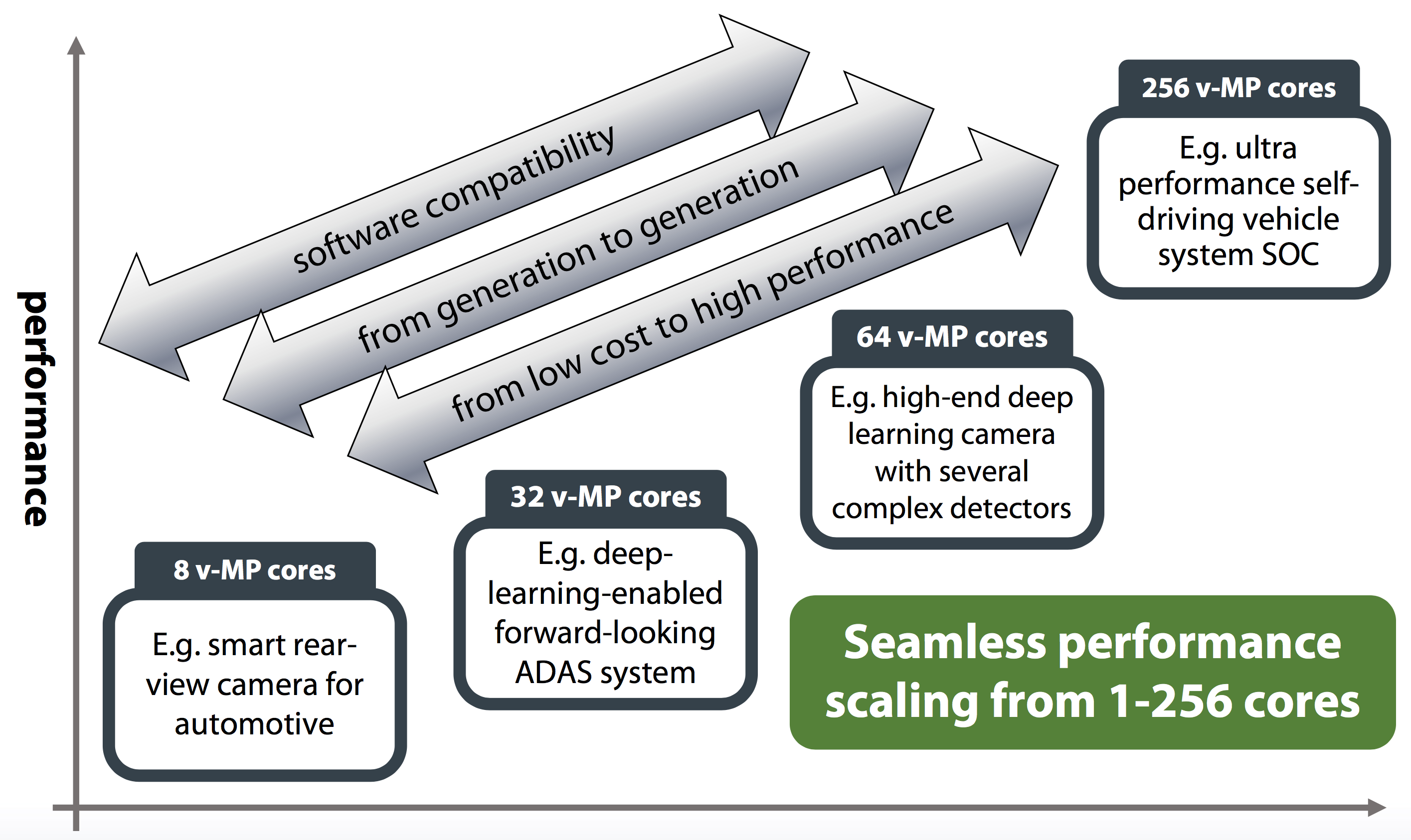
The peak number of cores per SoC has also grown significantly; whereas a high-end design in the v-MP4000HDX generation contained eight v-MP cores, Jacobs believes that modern SoCs are scalable up to 256 v-MP6000UDX-based v-MP cores (Figure 2). Both higher transistor counts and the higher layout efficiency videantis achieved with the v-MP6000UDX versus the v-MP4000HDX predecessor, Jacobs notes, are key to delivering high core counts in cost-effective SoC implementations.

Figure 2. v-MP6000UDX product implementations scale up to 256 v-MP core counts, targeting a range of computer vision applications.
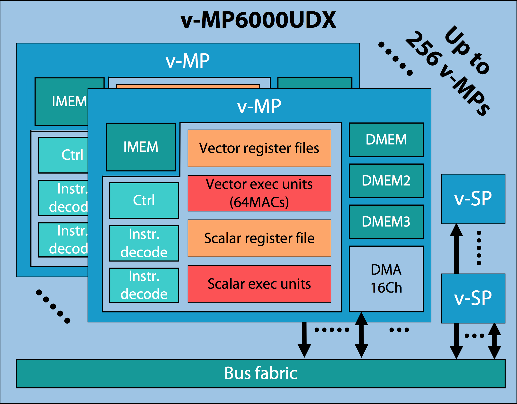
Higher MAC unit count potential translates to little-to-no practical performance improvement, however, in the absence of corresponding enhancements in connectivity, on-core and on-chip memory, and other critical subsystems. Unsurprisingly, therefore, these additional factors have gotten plenty of attention from videantis' architects, too (Figure 3). In addition to the local instruction memory, 4 KBytes of first-level data memory (DMEM) and up to 8 KBytes of level 2 DMEM, the v-MP cores in the new v-MP6000UDX architecture include up to 256 KBytes of DMEM3. The various-sized distributed and hierarchical memory blocks also have varying random and sequential access latencies and transfer rates, as well as varying bus widths and types of function units to which they're directly connected within the core.

Figure 3. A comparative abundance of both embedded memory and interconnect resources is also key to the v-MP4000HDX-to-v-MP6000UDX evolution.
Expanded intra- and inter-core connectivity strives to ensure that data flows through each core's memory, computation and other function blocks, as well as through the SoC containing the core(s), in an efficient fashion. Each core's interface to the inter-core bus fabric includes a 16-channel DMA controller. And the multi-core system design can also optionally support multi-bank on-chip memory to provide external system memory bus bandwidth relief.
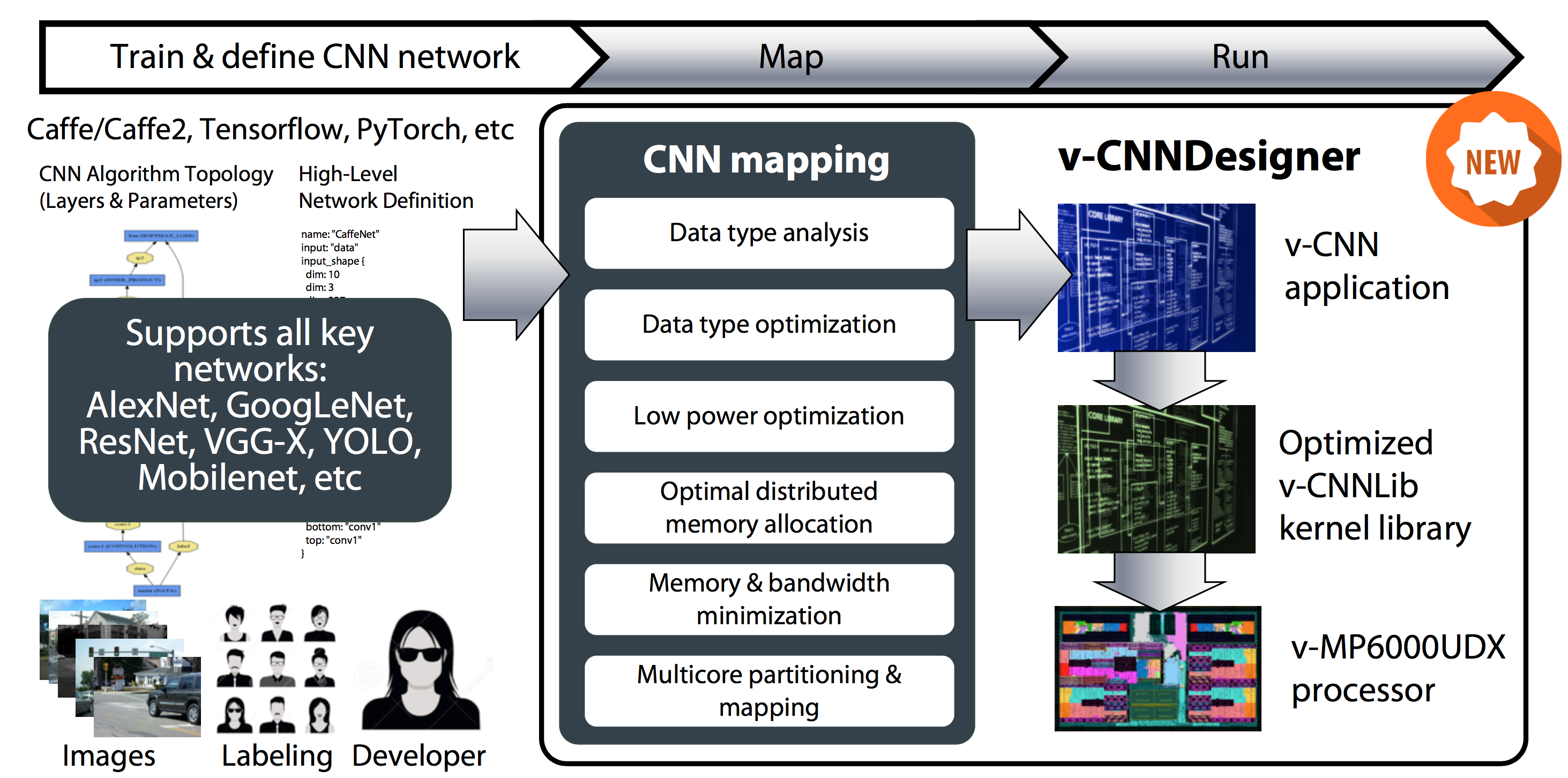
Conceptually similar to its deep learning acceleration core competitors, videantis has developed the Eclipse-based v-CNNDesigner toolset, which maps trained networks to the v-MP6000UDX architecture in a parallelized and otherwise optimized manner (Figure 4). Caffe and TensorFlow deep learning frameworks are currently supported, with Caffe2 support planned and other frameworks under consideration based on customer demand.

Figure 4. The v-CNNDesigner toolset ports neural networks designed and trained using frameworks such as Caffe or TensorFlow to run efficiently on videantis' cores.
The v-MP6000UDX instruction set architecture is backwards compatible with that of the v-MP4000HDX. Although v-CNNDesigner currently supports only the new core architecture, Jacobs notes that it would be conceptually possible to back-port the toolset to also support v-MP4000HDX, should a customer with more modest inference needs desire such architecture flexibility. The architectures's instruction set has been extended in the v-MP6000UDX generation for expanded acceleration support when processing all layers of a convolutional neural network (specifics are available under NDA, according to Jacobs).
The v-MP6000UDX architecture also retains support for the v-MP4000HDX's optional low-latency v-SP cores, one per image channel, for 8K resolution, 60 fps video encoding, decoding and transcoding using codecs such as H.264, still and motion JPEG, the Google-championed WebM and WebP, and Microsoft's Windows Media. v-SP cores find use when, for example, transferring image data from each camera in a vehicle to a centralized processor over an automotive Ethernet bus, or for archiving purposes.
Jacobs estimates that the v-MP6000UDX family will run at approximately 1.5 GHz peak on the 16 nm process node, across all possible core count and combination configurations. He declined to provide silicon area or power consumption estimates for v-MP6000UDX, and also demurred when asked to supply comparative speed, area and power estimations for v-MP4000HDX on the 16 nm process node. Jacobs generally noted, however, that v-MP6000UDX features such as fine-grained clock gating and a large number of per-core vector and scalar register files (the latter intended to keep data "local" as much as possible) were included specifically with low power consumption in mind. Both the v-MP6000UDX architecture and v-CNNDesigner toolset are now available for licensing.


Add new comment