With the proliferation of deep learning, NVIDIA has realized its longstanding aspirations to make general-purpose graphics processing units (GPGPUs) a mainstream technology. The company's GPUs are commonly used to accelerate neural network training, and are also being adopted for neural network inference acceleration in self-driving cars, robots and other high-end autonomous platforms. NVIDIA also sees plenty of opportunities for inference acceleration in IoT and other "edge" platforms, although it doesn't intend to supply them with chips. Instead, it's decided to open-source the NVDLA deep learning processor core found in its "Xavier" SoC introduced last fall.
In a recent briefing, Deepu Talla, NVIDIA's Vice President and General Manager of Autonomous Machines, explained that the company's open-sourcing decision was driven in part by the realization that the more deep learning inference that’s done in edge devices (regardless of whether this processing takes place on NVIDIA silicon), will also expand demand for cloud-based training of deep learning models, which is often done on NVIDIA's platforms. However, the number of processor architecture options for edge-based inference processing is large and still rapidly growing. According to Talla, the resultant inference architecture diversity threatens to stall overall market growth, although NVIDIA's claims may overstate the reality of this fragmentation's effects. Regardless, NVIDIA decided to encourage consolidation by openly licensing the NVDLA core integrated in the Xavier chip, which is intended for ADAS and autonomous vehicles and is currently scheduled to begin sampling next year both standalone and as part of the just-introduced Pegasus processing module (Figure 1).

Figure 1. NVIDIA hopes to counteract today's deep learning inference processor fragmentation, to the market benefit of its deep learning training processor business, by open-sourcing its internally developed inference processor core.
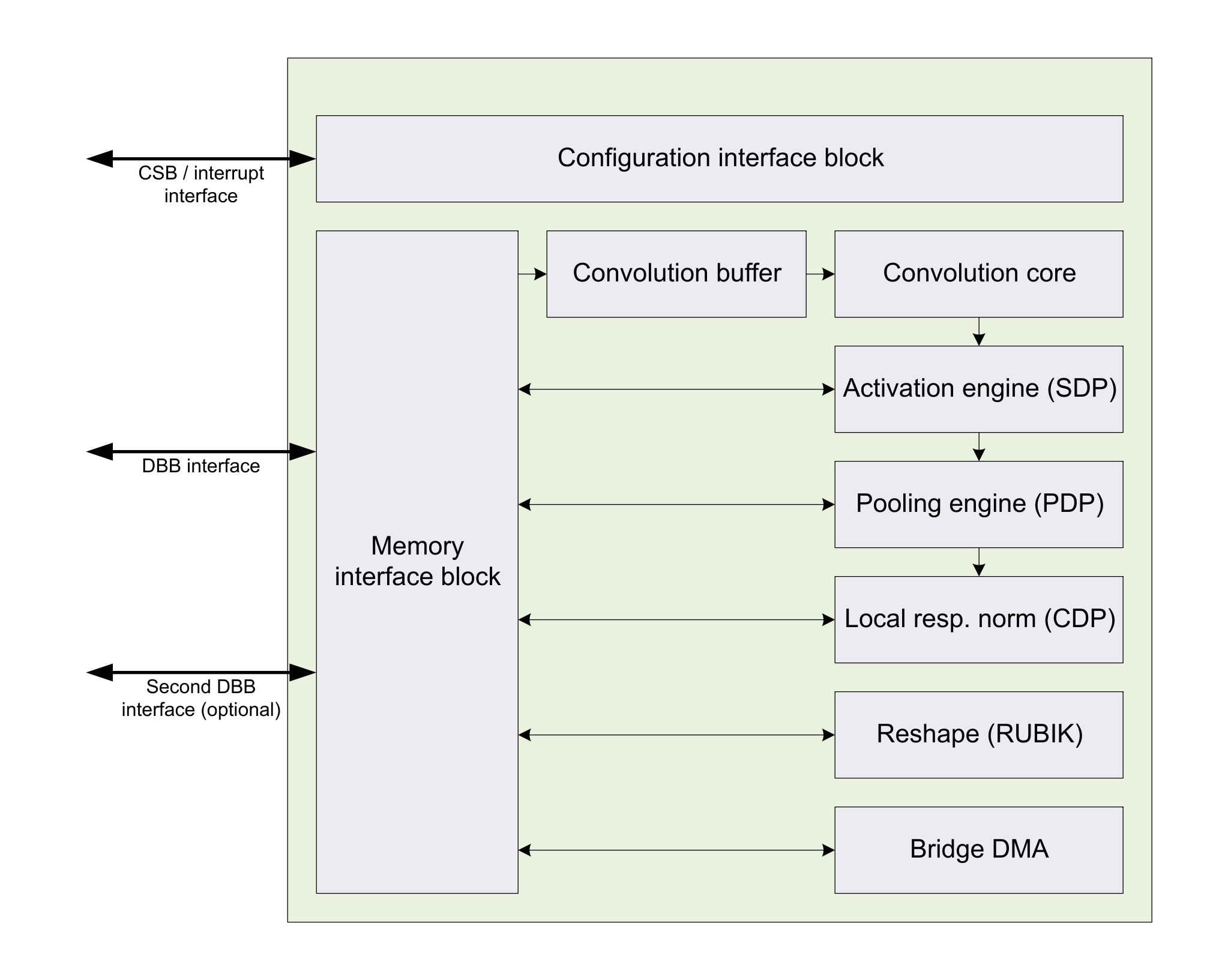
NVIDIA's website contains an abundance of information on NVDLA, with more to follow as the company continues executing its roadmap. Each 16-bit fixed- or floating-point multiplier-accumulator (MAC) in the core can alternatively be configured as two 8-bit fixed point MACs. The core includes an AXI interface to system SDRAM; an optional second AXI bus supports a supplemental local SRAM array. Additional core interfaces include the CSB (Configuration Space Bus), a synchronous, low-bandwidth, low-power, 32-bit control bus used access the NVDLA (slave) configuration registers and easily converted to AMBA or any other system bus via a simple "shim" protocol translation layer, and a 1-bit level-driven interrupt asserted when a task completes or an error occurs. And both cores, along with the generalized modular open source final version that is scheduled to succeed them next year, will be supplied by NVIDIA in both Verilog HDL (for simulation and synthesis) and TLM SystemC simulation formats.
NVDLA overview documentation, supplemented by in-depth specifications, provides area, performance and power consumption estimates for example core permutations at various MAC counts (Table 1). Note that, to quote NVIDIA's literature, the estimates assume that "no on-chip SRAM is used," although "on-chip SRAM would be beneficial if available SDRAM bandwidth is low." Note, too, that while the estimates assume a 1 GHz operating frequency for the core, the maximum clock speed at various process nodes has yet to be definitively determined.
| MACs | Convolution buffer size (KBytes) | SDRAM bandwidth (GBytes/sec) | Silicon area (mm2, 28nm) | Silicon area (mm2, 16nm) | Int8 ResNet-50 inference performance (fps, 1 GHz) | Power Estimate Peak / Average (mW, 16nm, 1 GHz) |
| 2,048 | 512 | 20 | 5.5 | 3.3 | 269 | 766 / 291 |
| 1,024 | 256 | 15 | 3 | 1.8 | 153 | 375 / 143 |
| 512 | 256 | 10 | 2.3 | 1.4 | 93 | 210 / 80 |
| 256 | 256 | 5 | 1.7 | 1 | 46 | 135 / 48 |
| 128 | 256 | 2 | 1.4 | 0.84 | 20 | 82 / 31 |
| 64 | 128 | 1 | 0.91 | 0.55 | 7.3 | 55 / 21 |
| 32 | 128 | 0.5 | 0.85 | 0.51 | 3.6 | 45 / 17 |
Table 1. NVDLA implementation examples and key forecast parameters.
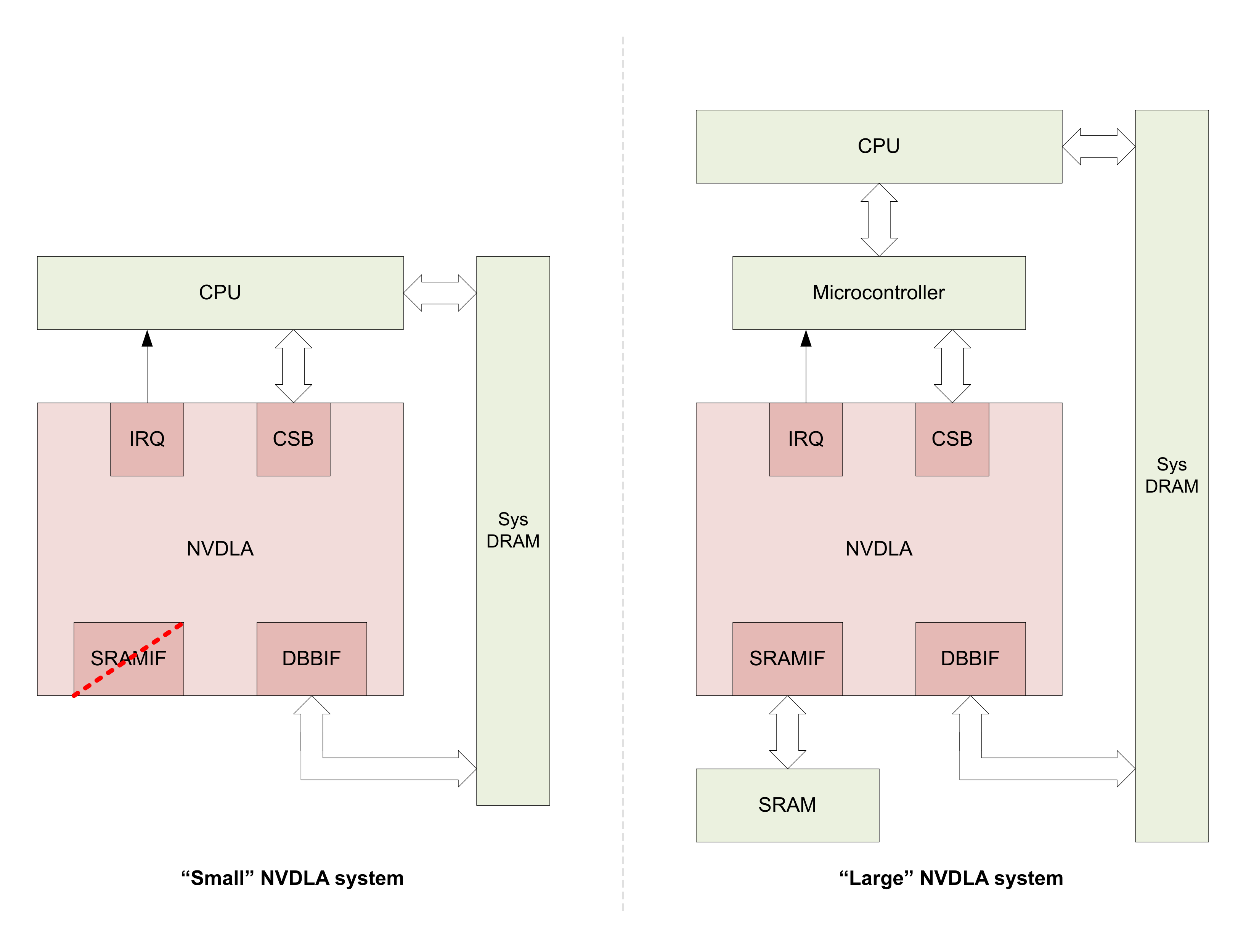
In addition to omitting the optional local SRAM, Table 1 also excludes the incremental area and power consumption (along with the potential inference performance boost) of a "headed" configuration that (as is done in Xavier) supplements the host CPU with a local microcontroller for core management purposes, versus a "headless" implementation that relies solely on the system processor for core control. NVIDIA has not announced what local controller architecture it's using in Xavier, according to Talla, and at this point does not plan to open-source its controller design. However, Talla noted, a number of other capable controller architecture options, such as those from ARM, Cadence, MIPS, Synopsys and (open-source) RISC-V, are also available.
NVDLA is comprised of "building blocks" which, in the core's final fully modular configuration, the company intends to be easily added and removed (as well as replicated) as needed in a given implementation to meet specific functional and performance requirements:
- Convolution Core – optimized high-performance convolution engine.
- Single Data Processor – single-point lookup engine for activation functions.
- Planar Data Processor – planar averaging engine for pooling.
- Channel Data Processor – multi-channel averaging engine for advanced normalization functions.
- Dedicated Memory and Data Reshape Engines – memory-to-memory transformation acceleration for tensor reshape and copy operations.
As NVIDIA's literature explains, "A system that has no need for pooling, for instance, can remove the planar averaging engine entirely; or, a system that needs additional convolutional performance can scale up the performance of the convolution unit without modifying other units in the accelerator." And the company plans to support both independent and fused operating mode programming options:
- Independent – When operating independently, each functional block is configured for when and what it executes, with each block working on its assigned task (akin to independent layers in a Deep Learning framework). Independent operation begins and ends with the assigned block performing memory-to-memory operations, in and out of main system memory or dedicated SRAM memory.
- Fused – Fused operation is similar to independent operation, however, some blocks can be assembled as a pipeline. This improves performance by bypassing the round trip through memory, instead having blocks communicate with each other through small FIFOs.
More generally, the hardware parameters planned to enable balancing area, power, and performance is extensive; see the NVDLA documentation for a list of these options.
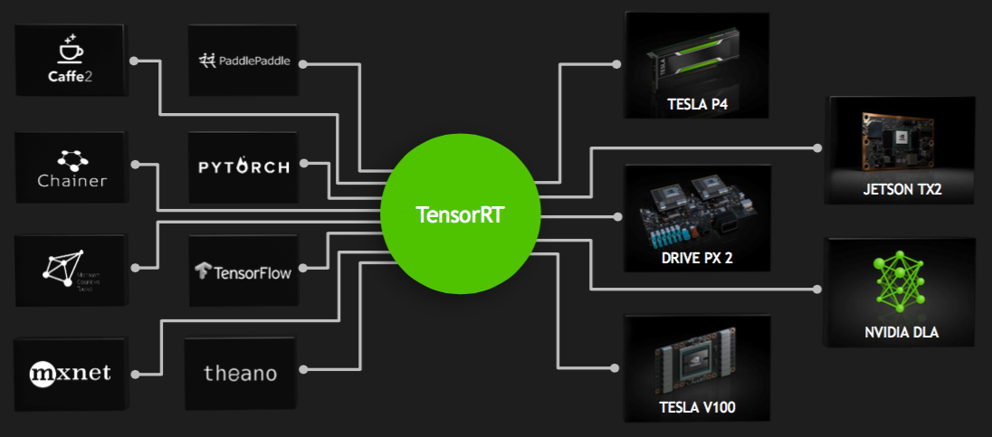
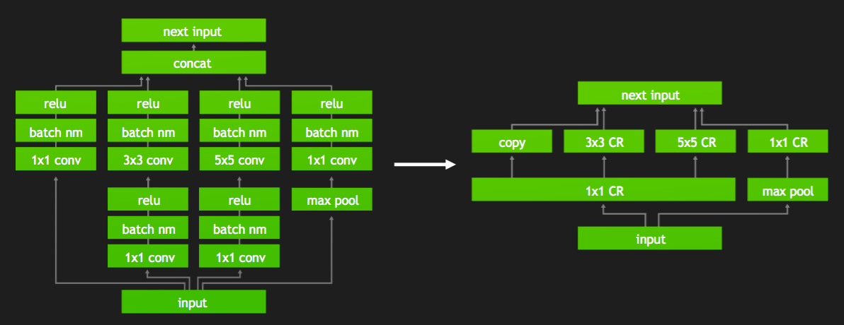
The company's software plans for NVDLA are equally thorough, albeit still somewhat in flux at this early program stage. The CUDA-based TensorRT compiler and run-time engine, recently upgraded to its latest v3 iteration, is the foundation toolset that NVIDIA intends for developers to use in converting a deep learning model into a NVDLA-optimized version, as well as to subsequently interact with the core at the operating system and application levels (translating into a long-term API "lock" that was likely also a factor in NVIDIA's open-sourcing decision) (Figure 2). Talla explained the current corporate thinking regarding compilation: the upfront parsing and intermediate-form compilation steps will remain closed-source long-term, while downstream final compilation and optimization algorithms will transition to open-source form so that developers can tailor them for specific core implementations. Similarly, the user and kernel mode drivers contained within the runtime environment will comprise a mix of closed- and open-source code, in both cases wrapped by a system portability layer, and with the intention of their being easily employed in both Linux and FreeRTOS designs as well as adaptable to other OSs.


Figure 2. NVIDIA's compilation and runtime software plans for NVDLA combine closed- and open-source modules and center on the company's TensorRT toolset (top), which both converts generic deep learning models into architecture and implementation-optimization versions (bottom) and enables operating system and application interaction with the core.
First to be publicly released (and currently available in "early access" form to initial adopters) is the full-featured version of the core as implemented in Xavier, with parallel AXI interfaces to both system SDRAM and local SRAM along with headed support for a local controller. Following it a quarter later will be a simpler NVDLA variant, headless and absent the local SRAM interface (Figure 3). The generalized modular version of NVDLA is currently scheduled for release in the first half of next year. NVIDIA's current published roadmap also documents a staged rollout of test benches, synthesis scripts, compilers and runtimes. The toolset will initially support the Caffe and TensorFlow frameworks but, Talla notes, as with other NVIDIA training and inference product platforms, a total of "eight or nine" frameworks are currently important within the company.

Figure 3. NVDLA reference design examples optionally supporting both local SRAM and a control microcontroller are planned in the near term, followed by a more general parameterized core version coming next year.


Add new comment