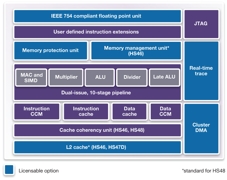
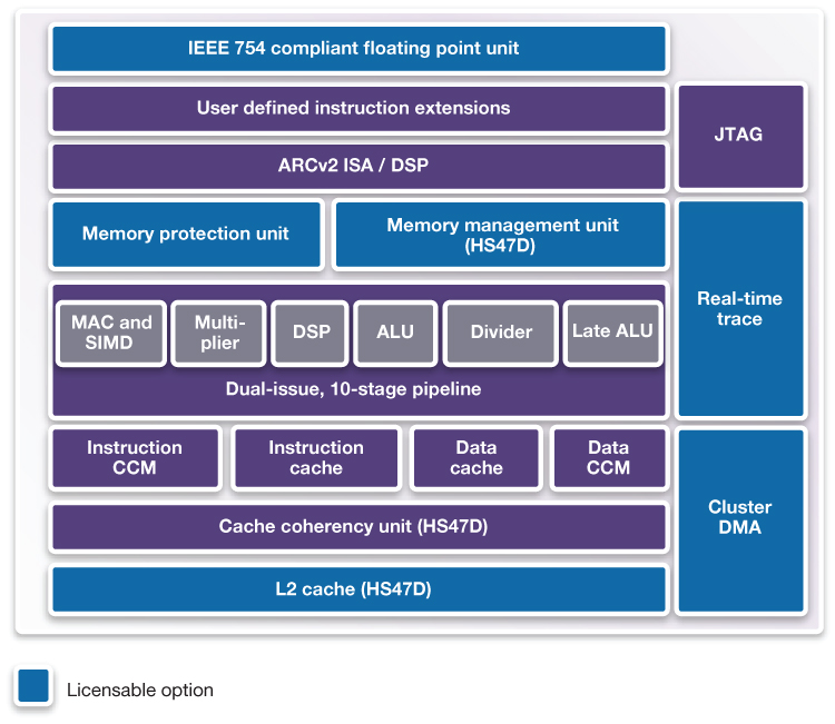
By adding a second front-end instruction decoder to the ARC HS3x high-end 32-bit RISC architecture, along with doubling the number of ALUs, Synopsys has created its latest ARC HS4x processor IP core family (Figure 1). The estimated performance increase over an ARC HS3x predecessor at the same clock speed can be as high as 40%, according to the company, with only modest die size and power consumption impacts. And via the inclusion of DSP enhancements akin to those initially launched with the mid-range ARC EMxD family, the HS3x-to-HS4xD (D=DSP) performance boost on code leveraging the associated expanded instruction set can be as much as 2x.


Figure 1. The superscalar ARC HS4x architecture can provide higher instruction throughput at a given clock rate versus the single-issue ARC HS3x precursor (top). DSP instruction set-supportive "D" variants deliver further computation enhancements (bottom).
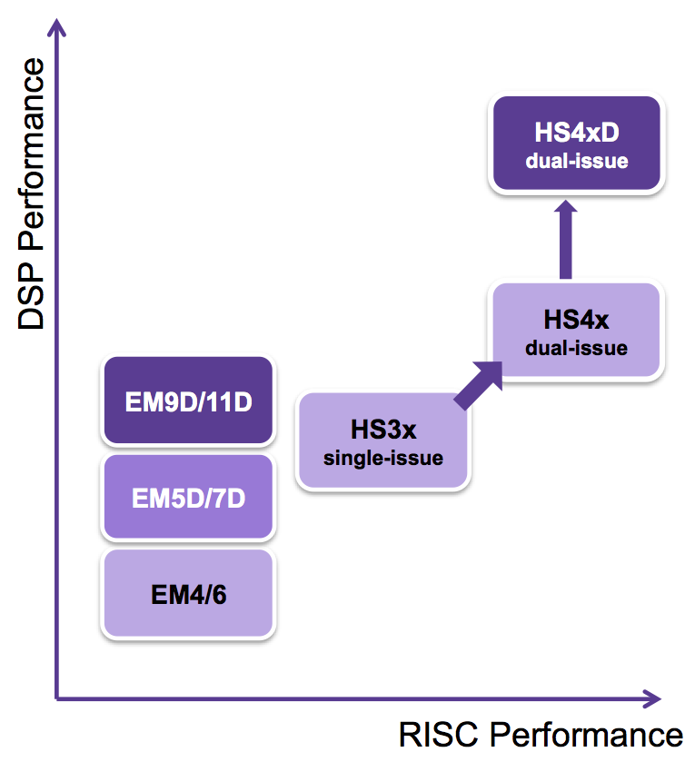
The ARC product line, initially promoted by ARC International beginning in the 1990s, was subsequently acquired by Virage Logic in late 2009. Less than a year later, Synopsys bought Virage Logic, including the ARC offerings. The ARC HS3x product line was initially unveiled in 2013; as the company's Senior Manager of Product Marketing, Mike Thompson, explained in a recent briefing, its differentiation from the mid-range ARC EMx product line (initially introduced in 2011) includes a deeper 10-state pipeline enabling higher clock speeds, optional dual- and quad-cluster multi-core support, and other options such as a MMU (memory management unit) for virtual memory capabilities with Linux and other advanced operating systems (Figure 2).

Figure 2. A deeper pipeline, translating into higher clock speeds, is one of several key differentiators between the mid-range ARC EMx and high-end ARC HS3x and new HS4x families. Both the ARC EMx and ARC HS4x families include members that support DSP processing enhancements.
Hardware options aside, ARC EMx and ARC HS3x are fully binary code-compatible, and this ARCv2 ISA (instruction set architecture) compatibility further extends to the new ARC HS4x offerings. With that said, Thompson noted that code specifically compiled for a particular architecture will still tend to be more efficient than that migrated unchanged from a prior architecture. To that point, ARC HS4x is dual-issue; by doubling up not only the front-end instruction decoder but also the number of early-stage (pipeline stage 6) and late-stage (stage 9) ALUs, ARC HS4x's superscalar approach can increase the average number of instructions processed per clock cycle, at the cost of approximately 50,000 incremental gates of logic.
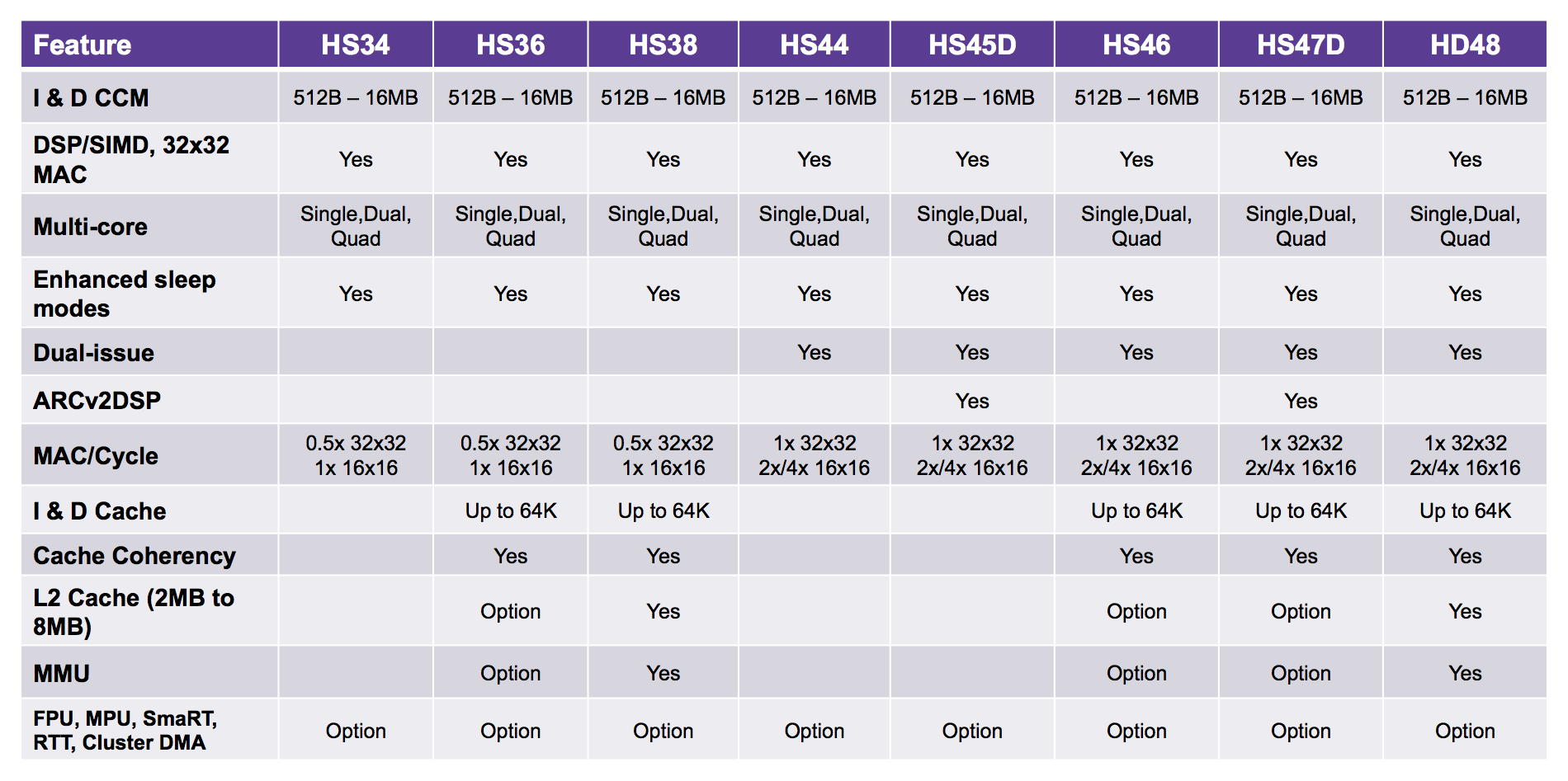
The availability of L1 and L2 caches varies with different ARC HS4x family members; the capacities of both these and the CCMs (closely coupled instruction and data memory arrays) are also user-configurable (Table 1). Other options include the aforementioned MMU, along with an IEEE 754-compliant FPU (floating point unit), a MPU (memory protection unit), a DMA (direct memory access) engine, and real-time trace capabilities. And as with other ARC core families, ARC HS4x also supports APEX (ARC Processor EXtension) technology, which enables licensees to add their own custom processor features via the hardware compiler found in Synopsys' toolset.

Table 1. Standard and optional features of various ARC HS3x and ARC HS4x processor core variants.
All ARC HS4x variants, along with their ARC HS3x precursors, integrate a separate processing pipeline for a 32-bit MAC, alternatively usable as dual 32x16 MACs and (for many operations) a quad 16x16 MAC cluster. With the ARC HS45D and HS47D members of the ARC HS4x family, both this MAC and the aforementioned ALUs are functionally enhanced to support the additional 150 software instructions found in the fuller ARCv2-DSP ISA. Synopsys' Thompson notes in these cases, the ARC HS4x's dual-issue architecture allows for the DSP-enhanced MAC and ALU pipelines (or other on-core resources) to operate concurrently, further boosting overall potential performance. Alternatively, if power consumption is the primary design constraint, an ARC HS4x- or HS4xD-based SoC is conceptually capable of delivering equivalent computing capabilities at lower clock speeds than that needed with an ARC HS3x-based SoC alternative.
Synopsys' Thompson positioned ARC HS4xD as primarily focused on the digital signal processing functions found in audio, speech, and wireless baseband applications. For all but the most rudimentary computer vision operations, conversely, a vision-tailored processing core such as the DesignWare EV6x is more appropriate, he suggested, with one of the company's CNN cores particularly relevant for deep learning-based applications. All five initial ARC HS4x/4xD variants are now available for licensing, with several of them already delivered to licensees and currently in design with tape-outs pending, according to Thompson. Forecasted ARC HS4 clock speeds range up to 2.2 GHz on a 28 nm process, or 2.5 GHz on a 16 nm FinFET process. The company plans to continue to offer the ARC HS3x family for more modest performance applications that value low silicon area and power draw; on 16 nm FinFET, for example, ARC HS3x cores can be as small as 0.06mm2 and consume as little as 30µW/MHz of power, he says.


Add new comment