
The cellular base station and its associated infrastructure topology have remained largely unchanged throughout the industry's history to date, although upgrades have periodically occurred to address the needs of evolving voice and data standards. Within each base station are beefy application-tailored, highly integrated DSPs from companies such as CEVA, Freescale, LSI, and Texas Instruments, all of which are regularly covered in InsideDSP. A beefy “backhaul” tether connects each base station to conventional wired networks for both voice and data traffic. And the base stations don't notably communicate with each other, save for managing call hand-off as particular cellular connections migrate from one tower's coverage region to that of another.
Similar architectures and topologies exist with smaller-footprint femtocell and picocell designs. And notably, the SoCs in today's cellular base stations are not x86-based; instead, they harness ARM- and Power-based general-purpose processors, alongside various DSP cores. Intel thinks it has come up with a superior base station approach, one that predictably embraces x86 at its nexus (at least for the present, until ARM's competitive cores are 64-bit capable). But the technique, called C-RAN (Cloud RAN), isn't (just) a power grab for additional market share, revenue and profit by the world's already-largest microprocessor supplier; its potential merits to service providers are equally notable.
Conventional base stations, the implementation of which is referred to as RAN (Radio Access Network), are expensive to construct, maintain and operate. They demand large amounts of electricity both to power their processing circuitry and to keep it cool. They must be outfitted for the peak voice and data demand that their coverage region will require, even though actual demand may notably undershoot this maximum threshold during a significant percentage of a typical day. Consider, for example, a downtown-located base station that is heavily used during weekday working hours but lightly used overnight and on weekends, when folks are at their residences in the suburbs. And the diversity of infrastructure equipment suppliers, which have equipment similarly based on a variety of silicon and software infrastructures, complicates the network integration task for cellular service providers.
In the alternative C-RAN approach, as the name implies, a notable amount of cellular processing is offloaded from each now-"dumber" base station to a centralized server rack. The approach not only reduces both the construction costs (assuming fiber optical "backhaul" already exists) and operation costs of each base station facility, it also allows for dynamic reallocation of virtualized processing resources from one base station to another as utilization shifts both intra- and inter-day. x86 CPUs can handle functions such as channel estimation and reception control with aplomb. Unfortunately, though, and in spite of ever-increasing and more robust multimedia instruction sets such as MMX and the subsequent various iterations of SSE (Streaming SIMD Extensions), they're not optimum for tackling FFT, MIMO decoding, de-mapping, turbo decoding and other functions that justify the DSP cores in conventional RANs' SoCs.
That's where ASOCS' MPUs (modem processing units), containing variants of the company's CR2100 DSP core, come into play. Communicating with one or multiple x86 CPUs over PCI Express, they act as co-processors (akin to a GPU) that enable a C-RAN scheme to adroitly handle a variety of 2G, 3G and 4G cellular voice and data protocols (Figure 1).
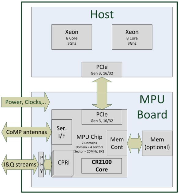
Figure 1. C-RAN migrates the bulk of cellular protocol processing out of each base station and into a common server farm, consisting of conventional x86 (or potentially, in the future, ARM) CPUs connected to DSP add-in cards via PCI Express links.
The MPU programming model is also GPU-reminiscent, akin to DirectX or OpenGL's abstraction of a computer's graphics subsystem. In this case, the ANSI C-based host CPU code controls the MPU by means of the MPL (Modem Programming Language) API (Figure 2).
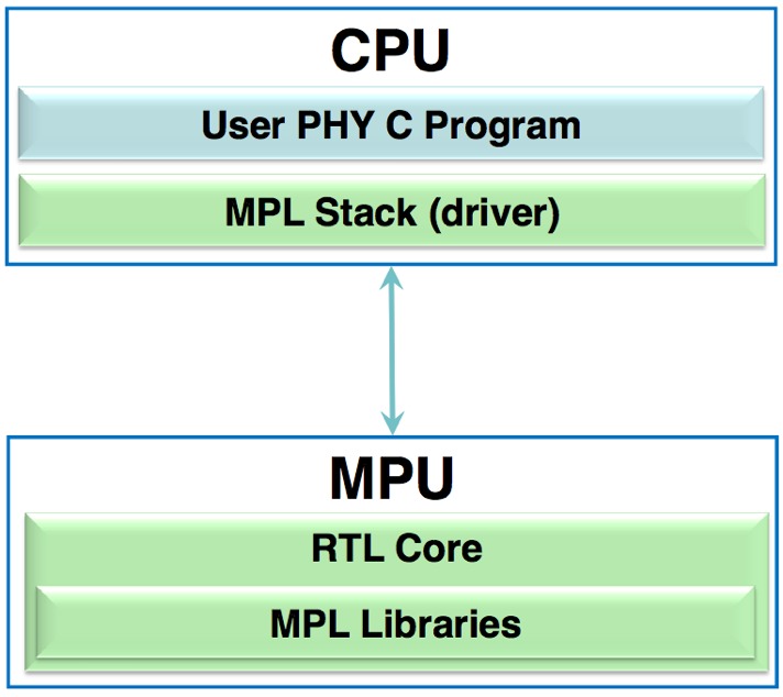
Figure 2. ASOCS' MPUs, like GPUs (via DirectX and OpenGL), are controlled via a C/C++ based API called MPL (the Modem Programming Language).
The following table summarizes some of the most common functions handled by the MPU and accessed via MPL, but is not comprehensive of the software library suite's span (Table 1).
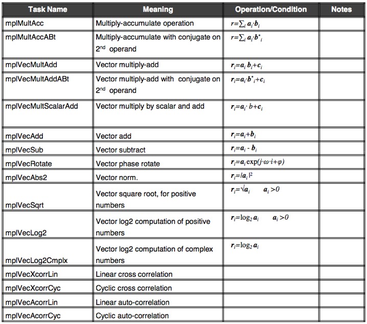
Table 1. This representative sample of the complete MPL library exemplifies the regular, arithmetic-heavy functions that the MPU (modem processing unit) offloads from the CPU.
And MPL is more than just a library, according to company CEO Gilad Garon. He claims that it allows for the definition of buffers, events, 3-D memory, etc., all providing programmers with a near-unlimited ability to define the modem within the framework.
Each domain-specific MPU derives from a heterogeneous many-core architecture that ASOCS refers to as ModemX. Depending on the particular protocols (2G, 3G, 4G), advanced features (MIMO, etc) and other capabilities to be implemented, including the number of simultaneous channels that require support (from femtocell to base station), the MPU integrates various types and numbers of PEs (processing elements), which execute MPL functions (Figure 3).
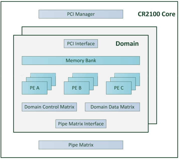
Figure 3. MPU silicon implementations are domain-specific, consisting of specific types and amounts of PEs (processing elements), along with inter-PE connection and other function blocks.
Possible PE functions, according to ASOCS documentation, include the following:
- FEC (decoder) PE: accelerator for decoding of turbo and convolution codes. The decoder supports all types of turbo codes (LTE, UMTS).
- Demapper PE: Extracts soft bit values from QAM signals, (LLRs), slicer decisions and slicing error values.
- Arithmetic PE: General-purpose arithmetic. Performs all the intrinsic arithmetic functions required by the MPU, like matrix multiplications, vector/scalar multiplications, windowing, and frequency correction.
- DFT/FFT PE: Orthogonal transform PE (FFT and DFT transforms). Frequency correction can be done on the input to the FFT/DFT unit.
- Logic_OP PE: Specialized for scrambling, PRBS generation, encryption solutions, and various encodings (e.g., convolutional and turbo). It operates on hard or soft bits. This PE can also perform interleaving and arithmetic operations.
- Data rearranging PE: This unit’s main purpose is interleaving and data manipulation. The unit can move/interleave large volumes of data, as well as handle IR (incremental redundancy), puncturing and simple decoding at high rates.
Each PE further subdivides into various combinations and numbers of APUs (Arithmetic Processing Units), programmable hardware tuned to specific mathematical operations.
In a welcome rarity, ASOCS provided a detailed case study design example, focusing on a 28 nm-manufactured MPU core. This particular variant is a C-RAN configuration, implementing the 20 MHz TDD (time-division duplexing) variant of UMTS (the Universal Mobile Telecommunications System 3GPP standard). Its MIMO configuration, supporting four spatial streams, consists of eight antennas each for receive and transmit subsystems. Peak bitrates of 300 Mbps download and 150 Mbps upload combine with simultaneous support for up to six sectors.
The number of per-sector PEs required (along with 2.7 Mbits of transmit-plus-receive memory) to implement the LTE design, which draws an estimated 1.087W of power, are as follows:
- PE_ARITH: 3
- PE_DEMAP: 1
- PE_FFT: 2
- PE_LOGIC_OP: 3
- PE_DECODER: 1
- PE_REORDER: 1
The following table details the silicon area (in mm2) required to fabricate the design (Table 2):
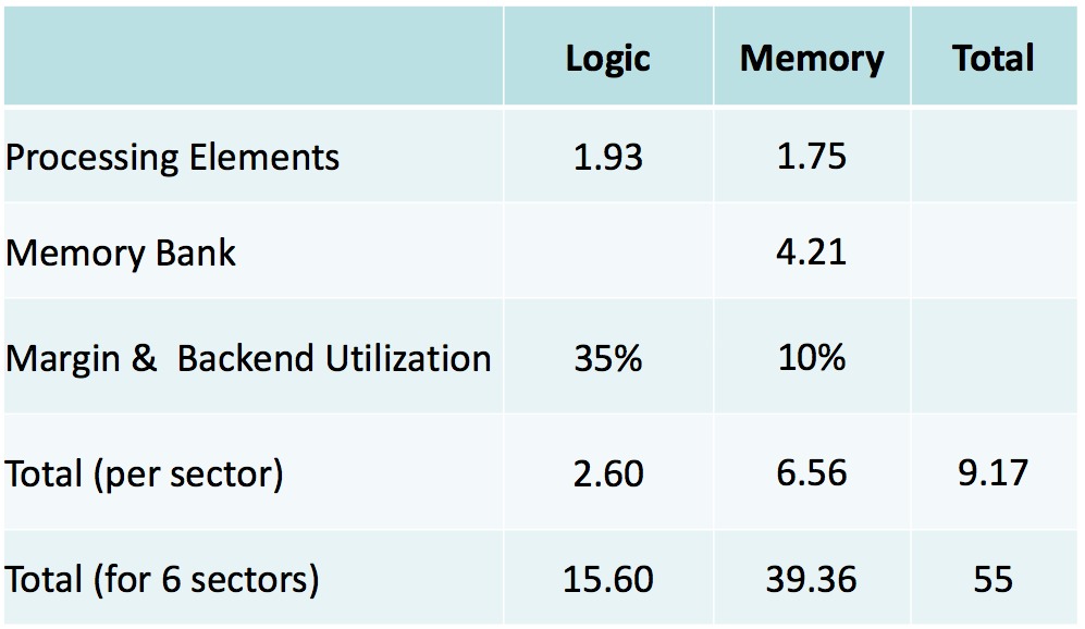
Table 2. ASOCs' MPUs, implemented in 28 nm ASIC processes, are compact in size.
ASOCS has been in existence since 2003; until a few years ago, according to Garon, the company was a vertically oriented provider of DSP ICs and associated software for handsets. SoC integration, coupled with supplier consolidation (due to both acquisitions and closures) compelled ASOCs to more recently redirect its strategy toward being an IP provider focused on infrastructure gear.
The C-RAN approach, with DSP virtualized in the common datacenter versus at each antenna, requires ultra-high speed and low latency connections between each now-"dumber" base station and the server farm that manages them. According to Garon, the predominant near-term market opportunity is therefore in Asia, which is comparatively fiber-rich. To wit, ASOCS reports that China Mobile has successfully tested MPUs implemented in FPGAs on C-RAN prototype systems. Pilot production of C-RAN equipment is reportedly underway, accompanied by an MPU implementation transition to lower-cost and lower-power-consumption ASICs.
While the technology world sometimes seems predictable and boring, breakthroughs such as C-RAN remind us that innovation remains alive and well. Admittedly, ASOCS' ease-of-programming claims, while compelling, have yet to be thoroughly tested. And, at least in the near term, C-RAN probably won't be implemented as quickly or as broadly as its advocates dream, for reasons such as insufficient fiber availability and the need for cellular service providers to first amortize existing equipment.
But C-RAN shows how fresh thinking, combined with Moore's Law-fueled ongoing improvements in cost, integration, performance and power consumption for both processing nodes and the connections between them, open the door to re-partitioning that can transform cellular and other seemingly staid industries alike. And others apparently agree: ASOCS just secured $3M USD in additional investor funding.
Add new comment