
Qualcomm has been evolving its in-house DSP core for many years. Originally developed for use in Qualcomm’s cellular modems, more recently it has also found use as an application co-processor, offloading multimedia tasks from the CPU in smart phones and tablets. Earlier InsideDSP articles covered the v4 "Hexagon" DSP core in mid-2012 and early 2013, along with the v5 Hexagon architecture later that same year. Now, with its Hexagon v6 DSP core, which will see its first silicon implementation in the upcoming Snapdragon 820 SoC, Qualcomm has deployed another path to high-speed math: wide vector extensions, which the company claims will particularly improve the performance of advanced imaging and computer vision tasks.
As review, "Hexagon" is the marketing moniker for Qualcomm's sixth-generation DSP architecture, also known as QDSP6. This sixth-generation architecture further subdivides into various evolutionary versions, with v6 discussed in this article being the latest. And this time, Qualcomm plans to even further subdivide the Hexagon v6 family based on the presence or absence of various features; the company calls the initial Hexagon v6 family member that we're discussing today the Hexagon 680.
As with prior designs (save for the initial v1), the Hexagon 680 is a multi-thread architecture. Hexagon v4 and v5 both supported up to three simultaneous threads, with v4 peak per-thread performance one third that of the master clock driving the core: 200 MHz per thread for a 600 MHz core, for example. Hexagon v2 was a six-thread design, with Hexagon v3 initially the same but later scaling back to handle four simultaneous threads. As Willie Anderson, VP of Engineering at Qualcomm, explained in early 2013, the fundamental reason for the per-version thread count variance involved review and optimization of trade-offs considering multiple contending variables:
- Code's ability (or lack thereof) to efficiently use all available core threads
- Core design complexity
- Core die size
- Maximum core clock speed, and
- Static and dynamic core power consumption
With respect to the architecture's arithmetic capabilities, Hexagon v5 (initially integrated in the then-flagship Snapdragon 800 application processor) focused on two primary enhancements:
- A newly added byte-operand option for vector operations, expanding on the existing 16- and 32-bit operand alternatives, and
- Floating-point arithmetic support, as an alternative to legacy fixed-point capabilities
It's also important to note upfront that Hexagon v5 evolved beyond its predecessors' elementary "round robin" thread-processing scheme to a more advanced approach known as DMT (dynamic multithreading). In this newer implementation, a not-yet-ready thread (due to a cache miss, interrupt, etc) is automatically skipped, leading to higher effective performance for the other threads at a given core clock rate.
Interestingly, the Hexagon 680 returns to the four-simultaneous-thread approach not seen since the initial v4 design, albeit carrying forward the v5 DMT enhancements. Since Hexagon uses a VLIW (very large instruction word) approach, each thread is able to execute up to four simultaneous instruction "slots" within in a given clock cycle; up to two of the four "slots" are also SIMD (single instruction, multiple data)-capable for even greater potential computation throughput. At a base level, each thread is scalar in nature, supporting both fixed- and (thanks to the previously mentioned v5 enhancements) floating-point arithmetic operations. Each thread "engine" contains a bank of 32-bit registers, and the scalar units all share common and variable-sized L1 data and instruction caches, along with a unified L2 cache.
The most significant new feature in the Hexagon 680, however, is its newly added HVX (Hexagon Vector Instruction) support. Scalar units can optionally hand over control to HVX vector processing "engines" found within the core (Figure 1). The two HVX units communicate with each other and the remainder of the core via the shared L2 cache, bypassing the L1 caches. Each HVX unit also includes a bank of 32 1024-bit registers that can be split into two banks of 32 512-bit registers. Thus with two HVX units, the Hexagon v6 can operate on 1024-bit vectors in up to two simultaneous hardware threads, or operate on 512-bit vectors in up to four simultaneous hardware threads. As with the scalar units, each HVX unit is a four-vector-slot VLIW architecture, allowing for a maximum of four vector operations per VLIW instruction packet.
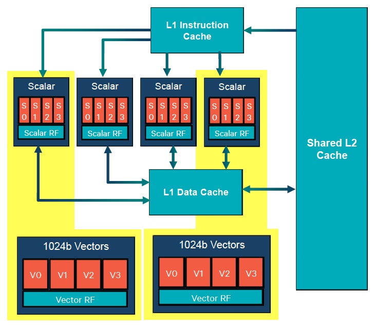
Figure 1. Threads supported by Qualcomm's Hexagon 680 DSP core can be directed to scalar or vector processing units (top); the latter store intermediate results and communicate with each other and the remainder of the core via a shared L2 unified cache (bottom).
HVX is fixed-point-only, supporting 8, 16 and 32-bit SIMD operands. According to senior director of product management Rick Maule, joined by senior marketing manager Adam Kerin in a recent briefing, omitting floating-point support resulted in a smaller and more energy-efficient design. Qualcomm also pointed out that many advanced image processing and computer vision algorithms do not require floating-point math, and that those that do can alternatively use the floating-point support built into the Hexagon v6 scalar units.
Each successive Hexagon generation tends to run higher peak clock speeds than its predecessor, thanks to both architecture and lithography advancements, and v6 is no different. Qualcomm claims up to 2 GHz clock rates with the Hexagon 680, translating into 500 MHz per-thread peak speeds (with all four threads utilized; higher on a per-thread basis if DMT is in play). However, the example benchmarks provided by the company run the Hexagon 680 at a slower 725 MHz clock rate (Figure 2). The benchmarks compare Hexagon v6 to a Krait-class quad-core ARM SoC running at 2.65 GHz, leveraging the available NEON SIMD instruction set capabilities. Note, too, that the claimed comparative power consumption metrics are core-only, not including SoC "infrastructure" logic, interconnect, system DRAM, etc.
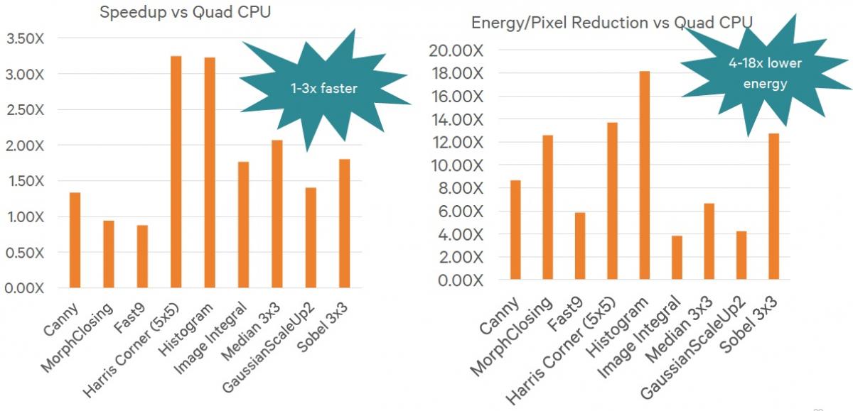
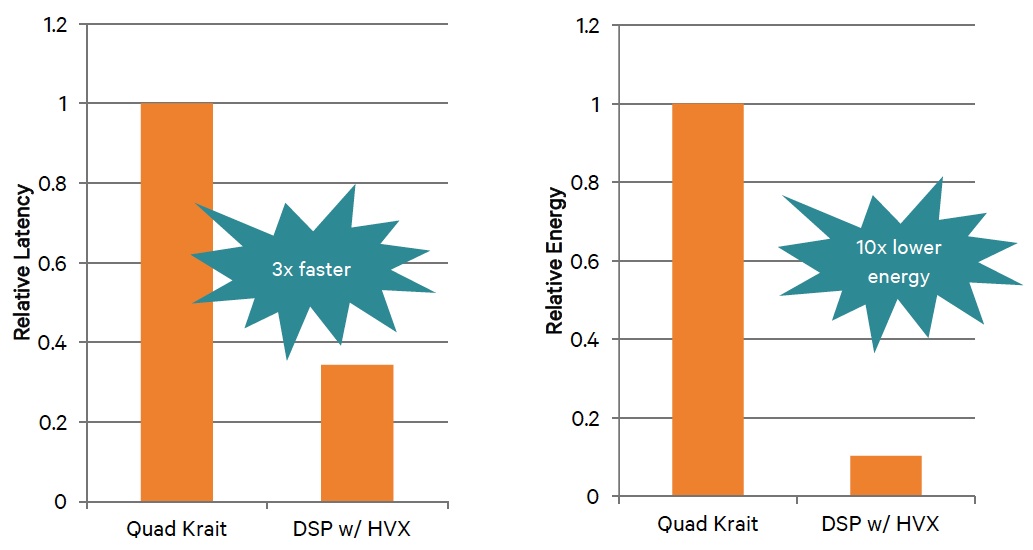
Figure 2. Qualcomm-supplied computer vision (top) and advanced image processing (bottom) benchmarks compare the Hexagon 680 to a quad-core, NEON-enabled ARMv7 CPU core running at nearly four times the clock speed.
The previously mentioned Snapdragon 820 SoC includes several other key advancements which are also capable of implementing embedded vision and imaging functions; the next-generation Kryo ARMv8 instruction set-capable CPU, for example, along with the Adreno 530 GPU and Spectra ISP (image signal processing) cores (Figure 3). Published details on these SoC elements are scant at this time; it's also important to note that the ISP is not developer-programmable. However, by virtue of their shared L2 cache scheme, the Hexagon 680 can act as a pre-processor for the ISP. And more generally, the heterogeneous computing capabilities delivered by APIs and development tools such as Khronos' OpenCL mean that imaging, vision and other similar algorithms will likely be partitioned across multiple cores, with tasks assigned to cores based on their respective strengths.
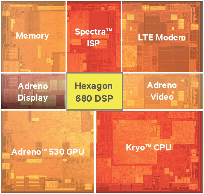
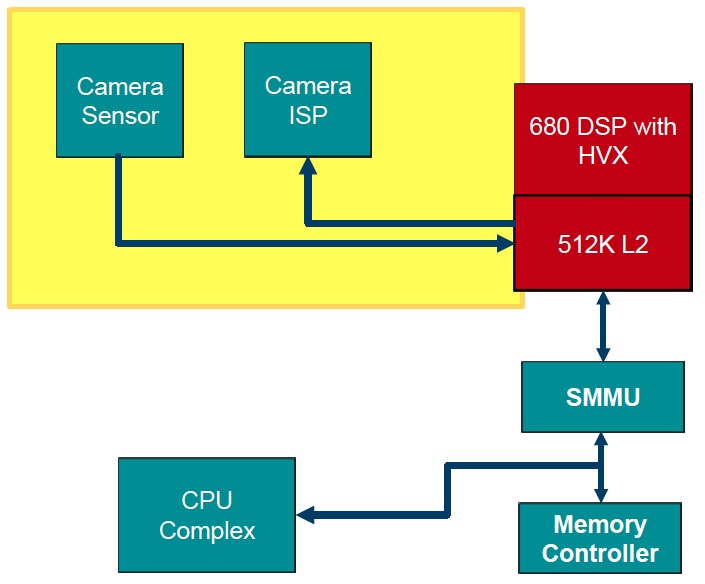
Figure 3. The Snapdragon 820, the first SoC to feature the Hexagon v6 DSP (top), contains numerous heterogeneous processing cores capable of communicating with each other and other application processors resources via cache and other means (bottom).
The previously discussed HVX vector extensions are optional. In the Snapdragon 820, they are included in the "Compute DSP," which functions as a co-processor for audio, speech, imaging and embedded vision functions. In addition, the Snapdragon 820 includes a second Hexagon 680 core within the “low-power island” sensor processing subsystem (Figure 4). This DSP is intended to deliver the sensor fusion capabilities that historically have utilized a separate "sensor hub" IC. And, as usual, there’s another DSP in the cellular modem, whose trendsetting LTE speeds Qualcomm recently touted. In the Snapdragon 820 SoC, this DSP is based on the earlier Hexagon v5 architecture, a decision made by Qualcomm to optimize time-to-market. Future Qualcomm SoCs, according to Maule, will likely transition to a Hexagon 600-series communications DSP.
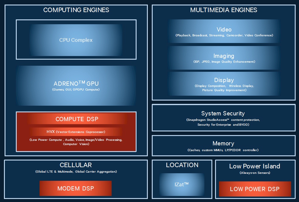
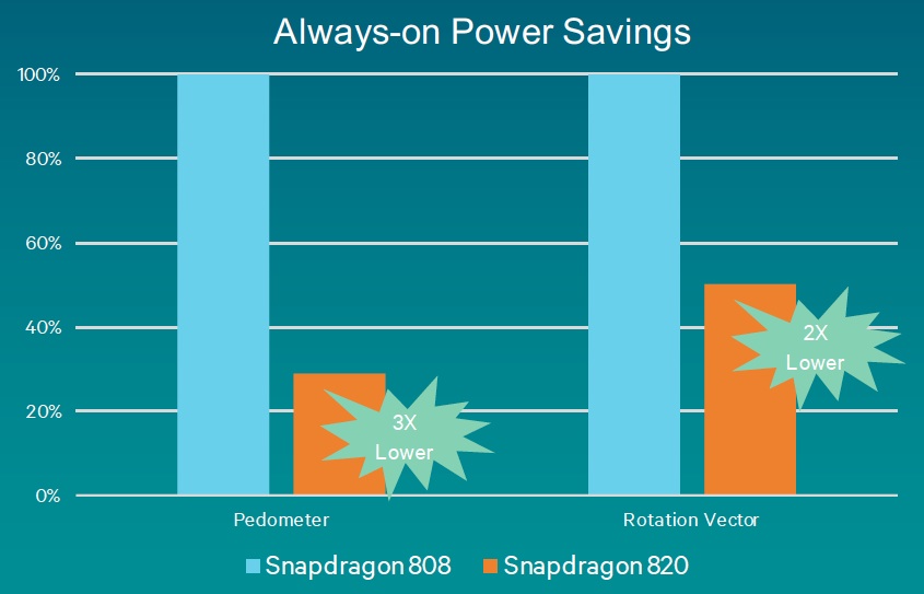
Figure 4. The so-called "Compute DSP" isn't the only v6 Hexagon core in the Snapdragon 820 (top). A second Hexagon v6 core is used for sensor processing functions. According to Qualcomm’s benchmark results, lower voltage operation combined with finer-grained voltage and clock gating and other architecture enhancements enable this DSP to deliver significant power savings versus its precursor (bottom).
The Snapdragon 820 has just entered the initial sampling stage; a simulator has been available for several months. Steadily expanding Snapdragon 820 sampling will continue through the remainder of this year, targeting early-2016 production smartphones, tablets and other systems. Qualcomm is confident that its steadily evolving compute DSP family will continue to give it defensible differentiation in the market versus competing SoCs. By January's Consumer Electronics Show or, at the latest, February's Mobile World Congress, we should have a better idea as to what degree they've translated this aspiration into tangible success.
Add new comment