
Back in September 2011, an InsideDSP article described a just-published analysis conducted by BDTI and sponsored by Altera, evaluating the viability of implementing complex hardware-accelerated single-precision floating-point functions on FPGA fabric. As I wrote then:
To date, FPGAs have been used almost exclusively for fixed-point digital signal processing functions. Although FPGA vendors have long offered floating-point primitive libraries, the performance of FPGAs in floating-point applications has historically been very limited. The inefficiency of traditional floating-point FPGA designs is partially due to the deeply pipelined nature and wide arithmetic structures of the floating-point operators, which create large data path latencies and routing congestion. In turn, the latencies can create hard-to-manage problems in designs with high data dependencies. The final result is often a design with a low operating frequency.
In the September 2011 study, BDTI leveraged Altera's DSP Builder Advanced Blockset and Quartus II RTL tool chain, Mentor Graphics' ModelSim simulator, and MathWorks’ MATLAB and Simulink tools to verify and evaluate an Altera-developed IEEE 754 floating-point Cholesky solver design example on two different Altera 40 nm FPGAs, the high-end Stratix IV EP4SE360H29C2 and mid-range Arria II EP2AGX125DF25I3. Among other outcomes, BDTI found the Altera Stratix IV EP4SE360H29C2 FPGA capable of performing 3,204 matrix inversions per second on matrices of size 240x240, running at a clock speed of 200 MHz.
As I also wrote then:
Moore's Law trends have benefitted FPGAs, leading to devices with more abundant logic (both generic and function-specific) and routing resources, made up of faster-switching and cooler-running transistors.
For this reason, Altera and BDTI recently revisited the study, focusing on two newer FPGAs, the high-end (and medium-size) Stratix V 5SGSMD5K2F40C2N device and the mid-range Arria V 5AGTFD7K3F40I3N device. The Stratix V FPGA used in this analysis is manufactured on the high-speed variant of TSMC's 28 nm process and features 345.2K ALUTs, 1,590 27x27-bit variable- precision multipliers, and 2,014 M20K memory blocks. The Arria V FPGA, fabricated on TSMC’s low-power 28 nm process, features 380.4K ALUTs, 1,156 27x27-bit variable-precision multipliers, and 2,414 M10K memory blocks.
The overall evaluation approach was largely unchanged from the earlier study, although a newer version of Altera's tool chain was used (v12.0 versus v11.0). To review the methodology, please reference the detailed description in the earlier InsideDSP article. Since the newer 28 nm FPGAs contained more hardware resources than their 40 nm precursors, BDTI and Altera decided to focus this evaluation on two multi-channel and otherwise more complex IEEE 754 floating-point design examples, a Cholesky matrix decomposition and a QR matrix decomposition using the Gram-Schmidt process. The QR decomposition is commonly used for any general m-by-n matrix, while the Cholesky decomposition is the preferred algorithm for a square, symmetric, and positive definite matrix, due to its high computational efficiency.
BDTI evaluated a total of eleven cases, spanning both matrix decomposition design examples, both FPGAs, and configurations with various combinations of channel sizes, matrix sizes and vector sizes. One of the Cholesky configurations was evaluated on both FPGAs, as were two of the QR configurations. Using the QR solver, the Altera Stratix V FPGA is capable of performing 315 matrix decompositions per second of size 400x400, running at 203 MHz and achieving 162 x 109 floating-point operations per second (GFLOPS). Both BDTI-verified design examples are available packaged with the DSP Builder Advanced Blockset tool chain, beginning with toolset v12.0. For additional information on this project, including:
- Detailed descriptions of the two BDTI-verified design examples
- BDTI's hands-on impressions of the Altera DSP Builder Advanced Blockset-based tool set design flow
- Additional clock speed, throughput, and resource utilization results for other QR matrix decomposition configurations, for various Cholesky decomposition configurations, and for the mid-range Arria V FPGA, and
- Error calculations for various single-precision floating-point FPGA implementations as compared to double-precision floating-point references
please download the white paper (PDF) from the Altera or BDTI web site.
With the 28 nm product generation, Altera and BDTI decided to expand the study beyond pure performance to comprehend power consumption and energy efficiency. Power and energy are becoming increasingly important in the selection of high-performance embedded processors, because many systems must operate in confined spaces, in mobile environments, or on battery power. However, a low-power processor is not necessarily energy efficient. Energy consumption is determined by multiplying power consumption by time. In many cases, a lower-power processor also provides lower performance, and its lower power may be cancelled out by the longer time required to complete a given task. And while a low-power processor may not provide enough performance, a high-performance processor may consume unacceptably high power.
Processor vendors commonly publish peak GFLOPS numbers. Similarly, energy efficiency is often quoted in terms of peak GFLOPS divided by power consumption (i.e. watts). These values assume that all floating-point functional units in the processor are running at the maximum clock frequency of the device. Such figures are usually very optimistic and do not reflect typical applications. In this analysis, therefore, BDTI and Altera took a different and a more realistic approach, measuring both floating-point performance and power consumption based on implementations of the Cholesky matrix decomposition and QR matrix decomposition design examples.
BDTI used two Altera hardware platforms for this evaluation; the DSP Development Kit, Stratix V Edition, and the Arria V FPGA Development Kit. The Board Test System, included in each kit's installation software download, communicates with the development board over a USB cable connected to the board’s USB-Blaster II unit. The USB-Blaster controls the JTAG chain on the board. The main DC power input on the board is stepped down via voltage regulators to supply power to the various power rails used by components on the board. The FPGA power rails are split from the supply plane by low-value, high-precision sense resistors, and 24-bit differential analog-to-digital converters (ADCs) are used to measure the voltage across these sense resistors (Figure 1). Each ADC communicates over a serial peripheral interface (SPI) bus with an Altera MAX V CPLD, which acts as the on-board system controller for various functions.
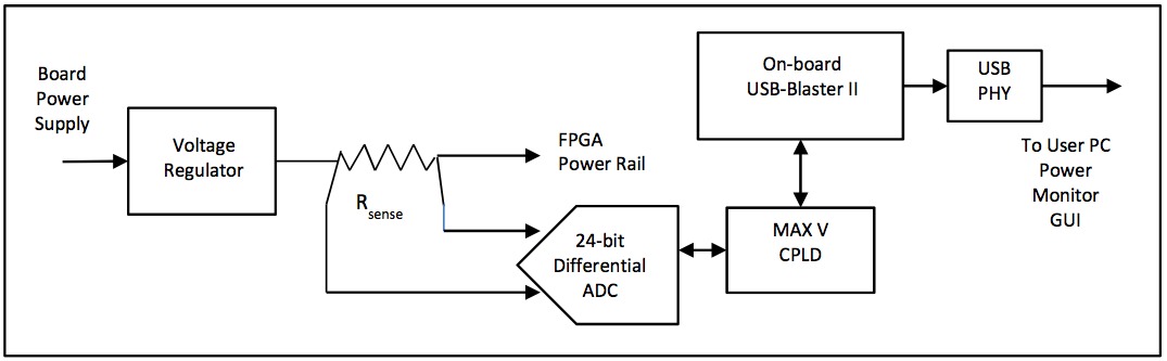
Figure 1. Each power rail of the FPGA's on-board power measurement circuitry communicates its power consumption to a common CPLD, which then passes along the data to a connected PC over JTAG.
BDTI monitored the current passing through nine power rails for the Stratix V FPGA and seven power rails for the Arria V device. In each case, the floating-point design example was running in continuous operation mode. Note that the total power consumption measured for each configuration includes the sum of power consumed on all the power rails of each FPGA. Although in many applications, including the examples tested in this study, some sections of the FPGA, such as the transceivers, are not actively used, they nevertheless contribute to static power consumption and were therefore included as part of the reported totals. In these examples, the FPGA core consumption ranged from 82% to 92% of the reported total power values.
The largest floating-point example evaluated was the earlier-mentioned 400x400 element QR solver on the Stratix V FPGA. Running at 203 MHz and processing 162 GFLOPS, the device achieved an energy efficiency of 6.2 GFLOPS/W while consuming 26 W. In comparing the two Altera FPGAs running identical floating-point design configurations, BDTI observed that although the Arria V FPGA has lower performance, it also has lower power consumption, translating into energy efficiency comparable to that of the Stratix V FPGA. Moreover, for similar computational performance (GFLOPS), BDTI observed that the Arria V FPGA achieves lower power consumption and higher energy efficiency than the Stratix V FPGA. These two observations indicate that the Arria V FPGA has both lower static and lower dynamic power consumption than the Stratix V device, reflective of its fabrication on the low-power variant of TSMC's 28 nm process.
For additional information on this project, including:
- BDTI's hands-on impressions of the two Altera FPGA development kits
- The measured voltages at each FPGA power rail, and
- Additional power consumption and energy efficiency results for other QR matrix decomposition configurations, for various Cholesky decomposition configurations, and for the mid-range Arria V FPGA
please download the white paper (PDF) from the Altera or BDTI web site.
BDTI's evaluation shows that the Altera FPGAs can achieve high computational performance executing complex floating-point applications, with power consumption low enough to enable their use in many power-sensitive embedded systems. As FPGAs continue to increase in size and provide increasingly optimized on-chip logic and memory blocks, and as their associated IP core libraries and software tool chains continue to mature, they will become increasingly attractive processing platform candidates for implementing various floating-point digital signal processing functions.
Add new comment